Tower Semiconductor provides its customers with advanced and differentiated design enablement capabilities that complement our specialized technology platforms.
Our industry-leading models, PDKs, and design tools empower customers with a strong competitive edge – enabling first-pass silicon success, optimized performance, and accelerated time-to-market.
Together, these best-in-class solutions enable a precise, efficient, and highly productive design process – empowering customers to meet the evolving challenges of integrated circuit (IC) development across a wide range of markets, including automotive, consumer, wireless and wireline connectivity, and industrial applications.
Cadence® Virtuoso® PDKs with interoperability with Keysight ADS for select flows
iPDKs for select processes to support Custom Compiler, ADS, and Tanner, EDA environments
Scalable models with RF/analog accuracy such as PSP for MOSFETs, MOSVAR, HiCUM for BJTs, R3 for resistors, HiSIM_SOI for RF SOI and HiSIM_HV for LDMOS devices
Scalable layout cells (p-cells), tightly coupled to the underlying models with features targeted for end applications enabling quick synthesis of layout blueprints
Monte Carlo statistical and mismatch simulation capability
PCM based models allowing design sensitivity analysis
X-Sigma – a unique process variation modeling tool enabling tradeoff of yield vs. performance
An industry-first scalable drift length LDMOS providing the highest level of SOA vs. performance
Design tools such as Inductor and Balun toolbox and foundry certified EM decks tailored to the needs of RF design from cellular to 5G and higher
Analog/RF friendly dummy fill and slotting solutions that help optimize the performance/yield trade-off
Extensive layout utilities to speed up gds synthesis time
Parasitic extraction and back-annotation integrated with model and layout features, including new capabilities for Flip-Chip packaging
Silicon verified substrate modeling capabilities embedded within the PDK
Advanced electrical checking for both devices and interconnects ensuring their reliability limits
Self-consistent electro-thermal simulation enablement via Keysight ETH and Cadence Legato in select flows
Reference Design Flows – silicon validated reference flows for power management and SOI switch designs highlighting proper use of PDK and models
3D-IC design enablement allowing for co-simulation, co-optimization, and co-verification of multi-die designs
PERC reliability checks for analog and automotive design – ESD, RESCAR constraint check, voltage aware propagation & DRC and P2P
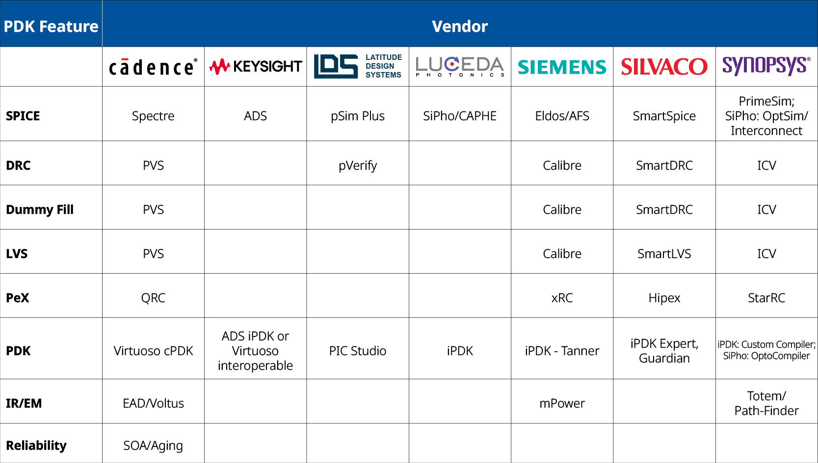
Best-in-class design enablement for silicon photonics with support for Ansys INTERCONNECT, Cadence CurvyCore, GDS Factory, Latitude Design Systems, Luceda, Siemens Tanner, Klayout based DRC from Spark Photonics, and Synopsys OptoCompiler, with Verilog-A models for electro-optic simulations in SPICE simulators
Tower Semiconductor Supported PDK Flows
Tower Semiconductor PDKs Partners
TowerJazz Provides PDKs for Keysight ADS
Submit the form below to be contacted by a Tower Semiconductor rep.
Tower Semiconductor websites place cookies on your device to give you the best user experience. By using our websites, you agree to the placement of these cookies. Click to Learn more