TPSCo has semiconductor manufacturing processes for 8-inch and 12-inch wafers at its fabs in Hokuriku, Japan (Uozu and Tonami).
TPSCo offers a broad range of advanced analog process technologies tailored to meet its customers’ precise specifications enabling the most cost-effective and versatile IC manufacturing solutions. With the cooperation of Tower Semiconductor, we work on developing new customers aiming at further business growth and expansion. TPSCo shall provide sophisticated and abundant process solutions for customers with keeping the excellent production quality
Uozu
Tonami
Arai
300mm (65nm)
200mm (0.35μm–0.15μm)
200mm (0.13μm–0.11μm)
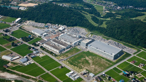
Operation started: December, 1984 Site Area: 250,413m2 Main Production Items: RFSOI, Power, Sensors, SiPho
Address: 800 Higashiyama, Uozu city, Toyama 937-8585, Japan
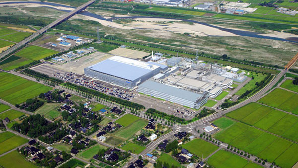
Operation started: October, 1994 Site Area: 228,446m2 Main Production Items: Analog, Power Discrete, NVM, CCD
Address: 271 Higashi-kaihotsu Tonami-city Toyama, 939-1312, Japan
Operation started: August, 1976 Site Area: 160,980m2 Main Production Items: Analog, CIS
Address: 4-5-1 Kurihara Myoko-city Niigata, 944-8555, Japan
Tower Semiconductor websites place cookies on your device to give you the best user experience. By using our websites, you agree to the placement of these cookies. Click to Learn more