

Embedded Non-Volatile Memory (NVM)
Embedded Non-Volatile Memory (NVM) allows enhanced functionality and higher levels of SoC integration.
Submit the form below to receive the PDF:
Tower Semiconductor provides NVM solutions with ultra-low power consumption, enhanced endurance, automotive grade retention, memory modules of different sizes with very fast programming, low start-up and read times, field programmability, and a high level of security. The NVM device, process and design solutions developed in Tower Semiconductor are protected by numerous US patents and does not lead to changes in the CMOS design kits and IPs. Combining the solutions internally developed and qualified on the Company’s CMOS production platforms MTP, FTP and OTP with the solutions of the leading external NVM IP vendors, Tower Semiconductor enables designed products that meet the diverse demands of analog and digital designers.
The Tower Semiconductor NVM portfolio is based on different physical principles (reference table below) and covers a wide range of memory densities and demands for endurance/retention performance, allowing flexible design configurations (e.g., trimming of reference voltages, currents, and amplifier offsets), faster time to market, vast advantages in product testing and yield enhancement.
Tower Semiconductor also provides a number of embefdded NVM implementation services including assistance in product design, verification, testing and qualification to ensure cost efficient and reliable integration of memory modules into customer products.
In addition, Tower Semiconductor collaborates with customers on joint development of emerging NVM solutions with a customer (e.g., low-cost charge trapping NVM, resistive RAM of different types, memristors, magnetic and ferroelectric memories, etc.) or transfer of non-volatile memories having high business potential for production in Tower Semiconductor fabs.
Memory technologies available in Tower Semiconductor
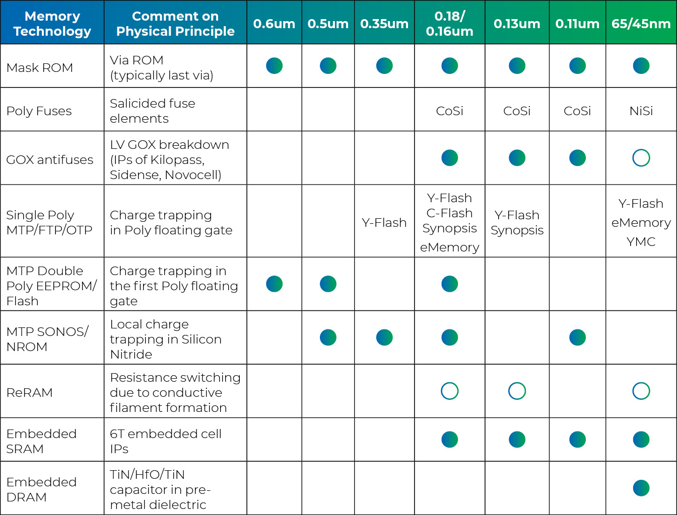
Broad NVM options exist in all Tower Semiconductor CMOS platforms. The Company also offers a variety of IPs of external vendors. To review our IP offerings, visit our IP solutions page.
The principle of operation of Y-Flash memory:
Separated transistors for the program/erase and the read-out. Asymmetric transistor principle (large drain capacitance to the floating gate 3D coupling geometry). Programmed by CHE, erased by BBT holes. Lower voltages compared with F-N NVM solutions (no need for special HV devices in the CMOS periphery). Record for single Poly EEPROM cell area (~ 3um2 in 0.18um DR). Cross-wise array organization with selects only for bit lines and word lines. Confirmed automotive (grade 0) retention performance.
Y-Flash modules for Power Management platform
Platform Features:
- “Flexible design” family
- Wide Vdd range: 2.5V–5.5V
- Flexible support of cuts in the range of 1K–16K
- Possible sub family modification to support area efficient 256b–1kb density range
- Possible modification to sub family of 32kb & 64kb
- Capabilities to support 10K cycles
- Capabilities to support automotive requirements
- Flexible CP to support different optimization schemes
- Possible adjustment to support 700V platform
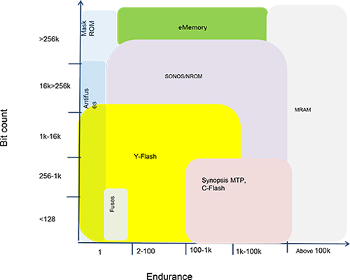
The below figure shows how the bit count-endurance is covered by different solutions provided by Tower Semiconductor technology: