


CMOS Image Sensor
Vast expertise in process and pixel customization enabling customer support in designing their pixel
of choice, meeting specific requirements and needs. Throughout the years we have brought to market many state-of-the-art customized design solutions for a variety of rising market applications.
Technology Highlights:
- Low noise global shutter pixels for industrial and machine vision sensors.
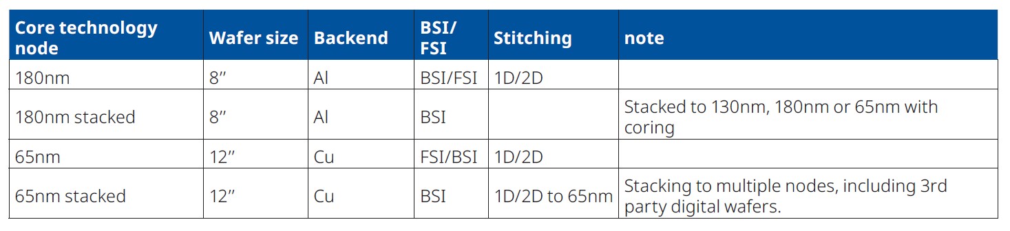
- Stitching technology with dedicated High Yield flows for large sensors and displays, up to one die per wafer.
- High density wafer stacking technology for BSI sensors with pixel level Cu-Cu connections.
Pixel Offerings:
RS – Rolling Shutter | GS – Global Shutter | SPAD – Single Photon Avalanche Diode | ToF – Time of Flight | FSI – Front Side Illumination | BSI – Back Side Illumination | Stacking – functionality split between imager wafer and readout IC
CA18 Imager Process Features
The Ci18N, N type photodiode and the Ci18P, P type photodiode process technologies add CMOS imager capability to the CA18 process family. The imager process capability is fully supported with pixel design instructions, imager design rule checks, and pixel layout versus schematic verification tools. The process design provides full optimization of pixel performance through the addition.
Platform Features:
Ci18N, NMOS 4T, 5T and 6T Photodiode
- Optimized for pixel pitch of 2.25 micron to 20 microns.
- High capacity photodiode with 50% higher linear full well than typical CMOS imager.
- 5T snap shot pixel.
- Zero lag.
- Process options for very high conversion gain (low floating diffusion capacitance).
- BSI process option.
Ci18P, PMOS 4T, 5T and 6T Photodiode
- Optimized for pixel pitch of 2.25 micron to 20 microns.
- Process options for very high conversion gain (low floating diffusion capacitance).
- Zero lag.
- Very low 1/f noise source follower.
Stitched Die Design and Process Support
- Subfield stitching and reticle stitching options.
- Stitch design pre-planning: Reticle and Wafer Level Floor-planning.
- Large die DFM recommendations.
- Local metal density analysis tool.
- Ongoing Title III program for Large Format Read-Out Integrated Circuit Foundry
- Improvement and Sustainability Program.