


TowerJazz 65nm 300mm Manufacturing Platforms:
The New Frontier for Highest Performance Advanced Analog Technologies
Febuary 27, 2019 | Category: Technology
300mm technology platforms offer many unique advantages such as ultra-low Rdson LDMOS transistors with high-density digital for high-performance power management ICs; ultra-low loss, high power linear RF switches and ultra-low noise RF LNAs for advanced front-end-modules (FEMs); and best-in-class global shutter pixel performance for ultra-high-performance cameras in the world. Integration of sub-65nm digital CMOS and optimized mask count allows exceptional die size reduction that improves product cost structure while providing rapid prototyping cycle times to bring best in class products to markets rapidly.
As a result, TowerJazz 300mm advanced analog technology manufacturing platform has become a platform of choice and a favorite “playground” for design and development of next-generation products for rapidly growing and emerging markets.
Power Management 65nm BCD
The power management IC is a fundamental building block for products that need long battery life and/or reduced power consumption such as a smartphone, a smart-wearable (e.g., watch), a tablet, or even your car’s LED highlights. Indeed, PMICs have become widespread in broad ranging consumer, automotive, and industrial applications that demand advanced power efficiencies to save energy and cost. The 65nm Bipolar-CMOS-DMOS (BCD) power management platform offers ultra-low Rdson power LDMOS transistors for 5V, 7V, 12V, and 16V operation, with exceptional Qgd values. The platform would soon be augmented to include power devices for 20V, 24V, and 30V operation, offering a rich portfolio of analog and digital IPs and eNVMs for smart power digital integration.

Through innovative engineering, TowerJazz’s 65nm BCD platform minimizes the mask count required to achieve desired performance, with dense digital density to achieve very small die size and highest power efficiency, making it the technology of choice for low voltage power management IC products operating up to 16V including load switches, DC-DC converters, LED drivers, motor drivers, battery management, analog, and digital controllers, and many more.
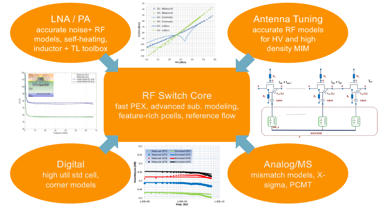
Radio Frequency – RF SOI 65nm
The RF SOI 300mm platform supplies a baseline to develop an innovative substrate extraction capability that is valid over a wide range of frequencies, operating bias conditions and uses existing features in industry standard extraction tools, addressing the emerging markets of RF communication and IoT. The radio frequency silicon-on-insulator (RF SOI) 65nm process enables the combination of low insertion loss and high power handling RF switches with options for high-performance low-noise amplifiers as well as high-density digital integration. It allows best-in-class metrics, by reducing losses in an RF switch, improving battery life and boosting data rates in handsets and IoT terminals, providing advanced solutions for next-generation 5G standards.
Our 65nm RF SOI technology provides accurate modeling of high-resistivity substrate material that is critical in optimizing the performance of RF switches for figures of merit such as insertion loss, power handling, and harmonic suppression. TowerJazz customers have successfully utilized this extraction capability for designing high-performance multi-throw switches and demonstrated excellent results.
Source: TowerJazz
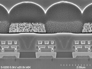
CMOS Image Sensor – 65nm Global Shutter
Using 65nm node for development enabled the design of a unique light pipe (a micro-optical structure that funnels the light directly into the photodiode) technology allowing half area pixel size as compared to other competing technologies, allowing our customers either increase resolution for the same cost or dramatically reducing their cost for the same resolution, while still offering state of the art functionality and superb angular response. The achieved structure provides global shutter pixels with outstanding Shutter Efficiency and Quantum Efficiency (QE) even at high ray angles (low F#s) thanks to the unique light funneling properties of the per pixel microlight pipe.
Based on this platform, we recently announced the release of our new Global Shutter (GS) pixel, vastly attractive to multiple end applications such as industrial and high-end machine vision, mobile face recognition and commercial applications, among others. This breakthrough achievement offers superb GS performance with a variety of pixel sizes down to 2.5µm, the smallest global shutter pixel in the world.
World’s previous smallest GS pixel, also achieved by TowerJazz, was 2.8µm in 2016 and was based on its 110nm platform. Using the 65nm technology node and optimization of our light pipe technology enabled us a further reduction of pixel size to 2.5um achieving these excellent performance characteristics.

As the global specialty foundry leader, we pride ourselves in aligning our long-term technology roadmap with the market leaders and market megatrends, to bring to market disruptive technologies for emerging applications for rapid commercialization. To that end, we are offering 300mm advanced analog platforms to provide our customers with best-in-class advanced technologies along with high-quality manufacturing capabilities.
To read more about our 300mm advanced technology offerings click here.