Process Design Kits (PDKs)
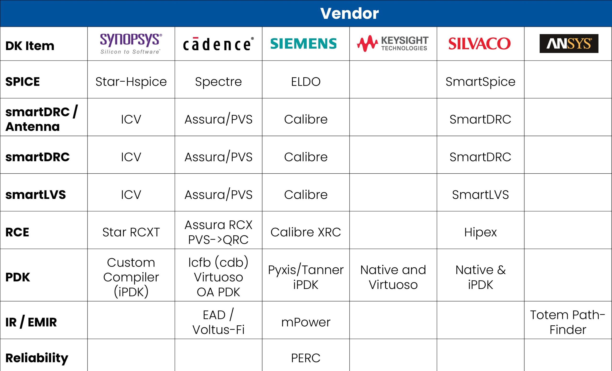
Tower Semiconductor PDKs offer a front-to-back integrated custom design environment that supports most major EDA vendors’ design flows.
Tower Semiconductor PDKs use sophisticated analytical techniques to warn designers when they have exceeded the electrical Safe Operating Area (SOA), allowing design optimization for reliability. In addition, silicon verified, highly scalable device models and robust physical design tools are available for up front design optimization. These powerful and efficient tools enable unprecedented accuracy in device models and Tower Semiconductor’s unparalleled customer support at every stage of the design flow ensures confidence in designs at near zero risk reducing time to market. Design kits support both PDKs and iPDKs.
Tower Semiconductor’s Process Design Kits Include:
- Advanced models such as PSP, MOSFETs and MOSVAR, HICUM for BJTs, R3 resistors and HiSim HV and SOI
- Scalable layout cells (pcells) for best design area efficiency
- Monte Carlo statistical and PCM based models
- Process variation modeling tool (X-Sigma ) that trade yield vs. performance
- An industry first scalable drift length LDMOS
- Scalable inductors Toolbox that provides silicon base
- Silicon verified substrate modeling capabilities embedded within the PDK
- Assert based SOA: Extensive “assert” based checking of electrical Safe Operating Area (SOA)
- Reference Design Flows
Tower Semiconductor Supported PDK Flows


