


Lights, Camera, (very fast) Action!
About the Global Shutter CIS technology that is changing the world
By: Dr. Assaf Lahav | March 16, 2020 | Category: Technology
At the heart of almost every camera we are using today, lies a CMOS Image Sensor (CIS). In most cases this CIS uses a so-called Rolling Shutter (RS) architecture to scan a scene. The scene information is captured and processed outside of the sensor line by line in a sequential way usually either from top to bottom or from bottom to top. When the scene involves moving objects or even if the camera is moving with respect to relatively still object or when a flash light is used is and not fully synchronized with the image scanning, the RS scanning may interact with the moving objects and create many types of image artifacts.
The evolution from Rolling Shutter (RS) to Global Shutter (GS) pixel technology
These well-known limitations of RS based sensors and cameras led image sensors engineers worldwide to design sensors with a more robust architecture, in which the image is captured simultaneously (or globally) over all the pixels of the sensor. This sensor architecture is known as Global Shutter (GS). The main drivers for developing GS sensors technology are:
(1) the growing industrial market where cameras are used to monitor or inspect fast moving objects in production lines (e.g. reading bar code labels accurately and fast);
(2) the automotive market where GS sensors are needed for creating better images from moving cars, automatic registration of cars license plates in highways toll stations, parking lots, real time monitoring of roads, and automatic speed registration and ticketing; and
(3) the last and biggest volume driver – the commercial applications like sports cameras, drone cameras and face recognition for edge devices, where a laser flash is used to project a grid of dots on one’s face and the camera needs to be fully synchronized with the projected pattern.
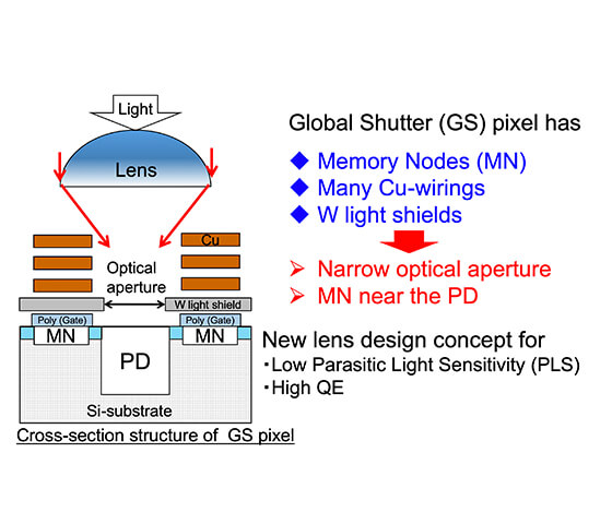
In a standard RS camera, each pixel in the sensor has a Photo Diode (PD) acting dually as a photo sensitive element and also as an information storage element for readout element. The pixel designer’s task is to maximize the number of photons that hit the photosensitive area while the readout is coupled (almost) directly to the information which is also stored in the PD. The GS pixel on the other hand is considered best-in-class when the PD is fully de-coupled from the read-out element. This often requires an additional element, called a Memory Node (MN), in each pixel which can store the relevant signal information until it is read out. Unlike the PD, which needs to be very sensitive to light and translate as many photons into electrons, the MN needs to be isolated as much as possible from incoming light in order to avoid any ‘mixing’ between information coming from two different frames. The stored image is the information from the previous frame which is now being read out, still line after line, while the new incoming photons should contribute to the signal of the current frame.
Comparison – a scene shot with RS pixel and GS pixel camera
Global Shutter Demonstration
Rolling Shutter Demonstration
Up until 2006, Charge Coupled Device (CCD) was by far the dominant GS sensor technology in the world, and CIS was relegated mostly RS architectures. Nowadays the CIS GS is widely accepted as the best solution for tracking and monitoring fast moving scenes.
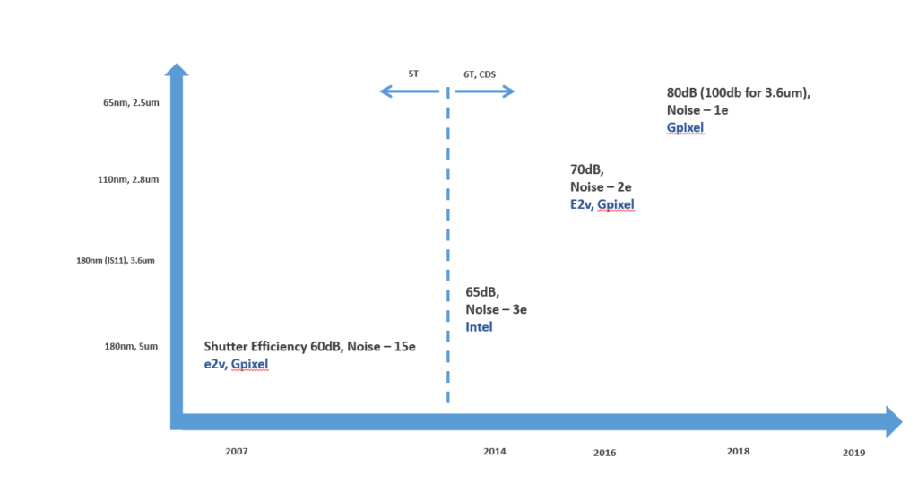
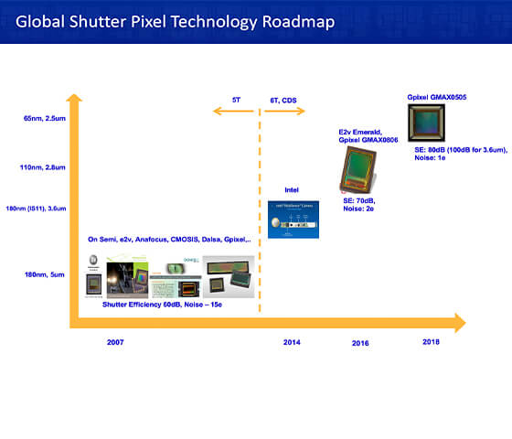
During that timeframe, Tower Semiconductor engaged with several breakthrough projects that increased penetration of CIS based GS sensors into the industrial market which was followed by strong demand from the Intelligent Transportation System (ITS) market and others. We continued to drive our roadmap for the best-in-class foundry solutions for GS sensor technology and best-in-class GS pixels in the world:
Gen 1: Our first generation of GS pixels went into production with relatively big (around ~5um) size, about ~20e of noise and a decoupling ratio between PD and MN of around 60dB. Despite being relatively lower performing than the best-in-class CCD pixels at that time, Tower Semiconductor’s GS technology was a huge market success, mainly because of much higher supported speeds at a higher resolution, which is hard to support using CCD technology. This initiated the shift in industrial cameras from CCD to CIS technology.
Gen 2: Our second-generation pixels were developed during our cooperation with Intel’s first RealSense™ IR camera. Originally intended for commercial applications like gesture control and 3D rendering, we adapted the technology in 2014 for industrial applications by combining 180nm periphery with 110nm metal lines in the pixel. This innovation enabled us to offer a pixel as small as 3.6um with noise of about 3e and rejection ratio of about 65dB (for the smallest pixel).
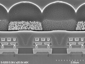
Gen 3: Our third generation of GS was developed using the 110nm Cu metallization technology in our TPSCo fab in Japan. In this version we had two embedded micro-lenses, that helped focus the light on the small diode area in this pixel, and also incorporated a tungsten shield (exactly like in best in class CCD), which helped in preventing light from reaching the MN, the pixel size was reduced down to 2.7um as well as a further reduction of the noise to 2e and increase in the rejection ratio to 70dB.
Gen 4: Our fourth, and the latest, generation of GS pixel was announced earlier this year. It is based on our 300mm based 65nm light pipe technology and improved tungsten shield, further enhancing the Gen3 performance. This technology allowed us to introduce the first 2.5um GS pixel with excellent performance (references IEDM, IISW), and are currently in the final development stage on further reduction of the pixel size to 2.2um.
Next-gen: Looking ahead, we are already developing our next generation GS pixel which will be based on Back-Side Illumination (BSI) technology. This generation would incorporate new innovations in process integration and device design to keep the MN isolated from unwanted light while maximizing light incidence on to the photo diode.
Tower Semiconductor Global Shutter Pixel Cross Section

To wrap-up, GS based sensors are enjoying a very rapid adoption in multiple markets and are experiencing total addressable market growth faster than the total image sensor market. Our pixel portfolio, combined with our capabilities, is recognized as the best-in-class GS offering in the world for any foundry, and we are working closely with market leaders to bring world-class products to market, or a theater near you!
For more information about our advanced CIS offering, please visit here.
Gen 1: Our first generation of GS pixels went into production with relatively big (around ~5um) size, about ~20e of noise and a decoupling ratio between PD and MN of around 60dB. Despite being relatively lower performing than the best-in-class CCD pixels at that time, Tower Semiconductor’s GS technology was a huge market success, mainly because of much higher supported speeds at a higher resolution, which is hard to support using CCD technology. This initiated the shift in industrial cameras from CCD to CIS technology.
Gen 2: Our second-generation pixels were developed during our cooperation with Intel’s first RealSense™ IR camera. Originally intended for commercial applications like gesture control and 3D rendering, we adapted the technology in 2014 for industrial applications by combining 180nm periphery with 110nm metal lines in the pixel. This innovation enabled us to offer a pixel as small as 3.6um with noise of about 3e and rejection ratio of about 65dB (for the smallest pixel).
Gen 3: Our third generation of GS was developed using the 110nm Cu metallization technology in our TPSCo fab in Japan. In this version we had two embedded micro-lenses, that helped focus the light on the small diode area in this pixel, and also incorporated a tungsten shield (exactly like in best in class CCD), which helped in preventing light from reaching the MN, the pixel size was reduced down to 2.7um as well as a further reduction of the noise to 2e and increase in the rejection ratio to 70dB.
Gen 4: Our fourth, and the latest, generation of GS pixel was announced earlier this year. It is based on our 300mm based 65nm light pipe technology and improved tungsten shield, further enhancing the Gen3 performance. This technology allowed us to introduce the first 2.5um GS pixel with excellent performance (references IEDM, IISW), and are currently in the final development stage on further reduction of the pixel size to 2.2um.
Next-gen: Looking ahead, we are already developing our next generation GS pixel which will be based on Back-Side Illumination (BSI) technology. This generation would incorporate new innovations in process integration and device design to keep the MN isolated from unwanted light while maximizing light incidence on to the photo diode.
Global Shutter Pixel Technology Roadmap
Dr. Assaf Lahav
CIS Research & Development Expert and Tower Semiconductor Fellow
Dr. Lahav joined Tower Semiconductor in 2001 and became a Tower Semiconductor Fellow in 2018. He has worldwide responsibility over the Company’s CMOS image sensor (CIS) technology offering. His research is focused on low noise global shutter technology, high resolution NIR imaging and back side illumination devices.