


Image Sensors: Leaving Fingerprints Everywhere in the Age of Consumer Data Protection and Security
By: Dr. Amos Fenigstein, Managing Director of CIS Research & Development, Sensors Business Unit | August 9, 2021
The fact that our fingerprints are unique has been known to us for more than a thousand years. But only after 1902, when Alphonse Bertillon solved a murder mystery and art theft near Arc de Triomphe in Paris, with a single fingerprint on a window frame, that fingerprinting became a fundamental tool of the detectives to identify criminals. Indeed, today, fingerprinting has become one of the most commonly used and reliable personal identification tools everywhere, not only for solving criminal cases but also for ensuring high security in conducting transactions over our smartphones. First introduced in high end smartphones, the fingerprint sensors very quickly became ubiquitous on every smartphone. While face ID sensors or retina sensors also provide the comparable levels of security, fingerprint sensors remain today the most common for personal identification, because of their lower cost, simplicity, and privacy considerations (some people are reluctant to use face recognition).
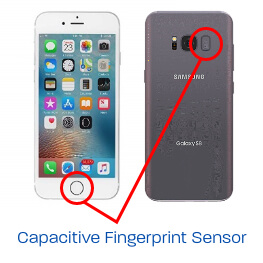
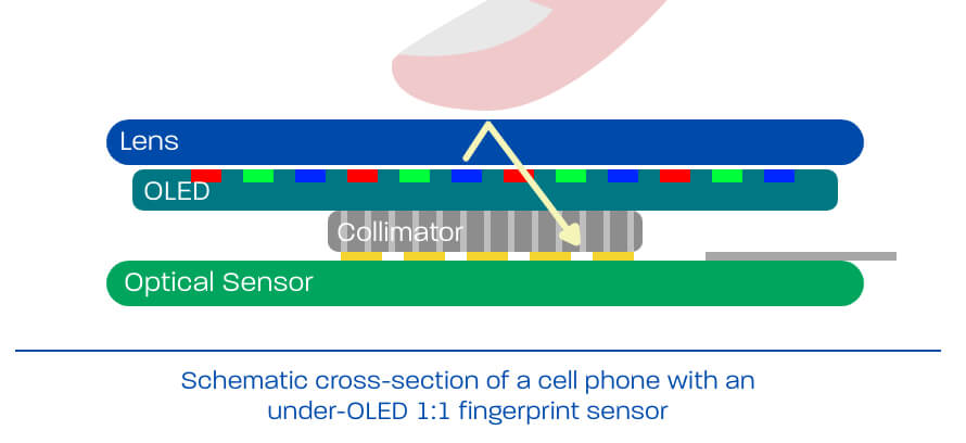
Indeed, the past several years has seen explosive growth of numerous companies as the demand sky-rocketed for fingerprint sensors that were specifically designed for implementation on the “home” button of every smartphone. Shortly after, the shift of cellular manufacturing companies to a full glass screen design without a home button created an interesting challenge to the implementation of a fingerprint sensor, because a capacitive fingerprint sensor required direct contact with the finger, and without the ability to have this direct contact, it made the capacitive fingerprint detection impossible. At first, an interim solution adopted by some smartphone vendors was to place the sensor on the backside of the phone but soon the solution proved to be very uncomfortable and not user-friendly. To overcome this challenge the designers introduced innovative optical based fingerprint sensors that, unlike capacitive ones, do not require a direct contact and function reliably under both LCD and OLED screens. Soon these optical fingerprint sensors are becoming ubiquitous because of their ease of integration with all-glass-all-screen display smartphones.
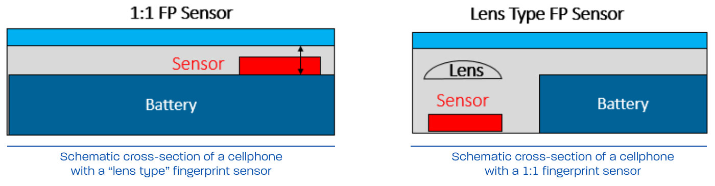
There are two major “under screen” optical sensors technologies:
- a lens-type sensor that uses a system lens and thus uses pixels the size of 5 to 6 microns to resolve the 50um features resolution in the fingerprint,
- a 1:1 sensor that does not use a lens and thus, requires large pixels, of around 50um.
The reason to use 1:1 sensors, although it is much larger than a lens-type and as a result are much more costly, is the minimum sensor height that can be achieved only with a lens-less sensor. Such small heights, as small as half a millimeter, is crucial for high end 5G smartphones, where there is only 0.6mm space between the battery on the back and the screen. The lack of lens, however, poses other challenges that drive the development of technology solutions to funnel the light into the pixels (collimator) as well as to filter out ambient light (tight optical filter), both increasing even further the cost of this type of a solution
Generally, the requirement from the underlying fingerprint technology is similar to those in other image sensors. High quantum efficiency is needed to cope with the constant starve for enough photons. Low dark current and low noise floor are essential for good signal to noise ratio, and both low noise and decent full-well are needed for a proper dynamic range.
These requirements, in addition to the required pixel size and other optical features such as an addition of a collimator and a tight spectral filter, makes Tower’s well established 0.18-micron platform on 200mm wafers the best fit for this application.
As mentioned above, the pixels required are rather large – around 5μm for lens-type, and tens of microns for the 1:1 sensors – the sweet spot of a 0.18 micron CIS platform. Process simplicity offers cost-effectiveness alongside super high performance. Beyond excellent 4T classical pixels, more sophisticated pixels are available, like pixels with “in-pixel memory nodes” (one or more), without adding kTC noise.
For the 1:1 sensor, Tower offers high-performing pixels with reduced masks, hence cost-effective for such big sensors. A special thick optical backend was developed to enable quality angle filters (collimators).
Below are figures of a cross-section demonstrating high SAG micro-lenses and the angular dependence curve of a filter implemented using this process.
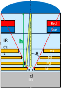
Cross-section of an angle filter implemented by a micro-lens and a set of apertures

Microlens-Aperture angle filter performance: Signal vs. incidence beam angle
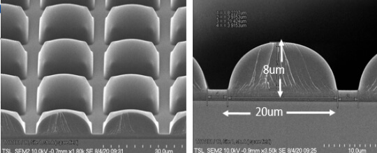
An array of elevated high SAG micro-lenses
Cross-section of an elevated high sag (8um) micro-lens
To summarize, fingerprint sensors are an essential part of cellular phones security features. Optical fingerprint sensors are an attractive solution, enabled on “all-glass-all-screen” smartphones with a convenient access to the sensor. Tower’s 0.18-micron CIS process offers a cost-effective high-performance solution for optical fingerprint sensors, both for lens-type and for 1:1 fingerprint, with special optical backend such as thick elevated microlenses acting as a collimator and a tight spectral filter to reduce ambient light noise.
Please visit here to learn more about all our CMOS Image Sensor technologies and much more.
Dr. Amos Fenigstein
Managing Director of CIS Research & Development, Sensors Business Unit
Dr. Amos Fenigstein is a senior director of R&D for image sensors in Tower Semiconductor since 2005. During these years Amos’s team developed a wide range of CIS pixel technologies, ranging from high end cameras and industrial fast global shutter sensors, to large X-ray sensor and SPAD devices. Amos has been with Tower since 2001 starting as device engineering manager. Before joining Tower, Amos managed a failure analysis team in Intel for its flip chip technology in the years 1998 – 2001. Prior to Intel, Amos worked for SCD on state-of-the-art MCT far infrared image sensors till 1998. Amos received his B.Sc., M.Sc. and D.Sc. from the Electrical Engineering Department of the Technion, Israeli Institute of Technology (D.Sc. in 1995 on Quantum Well IR sensors), where he lectures on CMOS and CIS technology to these days.